AI-Driven PCB Pipeline
Intent in English → SKiDL circuit → KiCad board → fab-ready Gerbers, with an LLM as the systems architect.
- Version
- v0.8 — AI-optimized fab-ready
- Reference boards
- 4 · up to 41 components
- Stack
- SKiDL · KiCad 9 · FreeRouting
- Backend
- Ollama · OpenRouter · Anthropic
Premise
Schematic capture and board layout are the two places electronics design still moves at human speed. The logic — what parts, what nets, what topology — is the part a language model is actually good at: it's reading datasheets, matching pin functions, and wiring up a netlist. The physical layout — where every footprint sits and how every track routes without crossing — is the part a model is bad at and a specialized solver is good at.
So this pipeline splits the work along that seam. You write the intent in English. An LLM acts as the systems architect and emits the circuit as code. Deterministic tooling compiles that to a netlist, places and routes the board, and exports a fab-ready Gerber package you can drop on JLCPCB or PCBWay. The interesting question the project keeps asking is how far up the complexity curve that division of labor holds.
- Reference boards
- 4
- Fab-ready
- 3of 4
- Largest board
- 41components
- Copper layers
- up to 4
The pipeline
Five stages, each owned by whichever actor is best at it. The LLM never touches geometry; the solver never invents a part. The handoff between them is a plain netlist.
- human
intent.md
high-level goal, in English
- LLM
circuit.py
hardware-as-code (SKiDL), with ERC auto-fix loop
- SKiDL
.net
logical connectivity
- solver
.kicad_pcb
placement + routing, AI-in-the-loop
- fab
Gerbers
DRC-gated, fab-ready zip
intent → circuit → netlist → board → fab · pipeline v0.8
The generator isn't a single prompt. intent.md → circuit.py runs a
three-example few-shot prompt with a per-IC pin-name catalog, then an
ERC → auto-fix loop: if the SKiDL build fails an electrical-rules
check, the error and candidate footprint suggestions get fed back to
the model, up to five times, until it compiles. Local Ollama is the
default backend; OpenRouter and the Anthropic API are there for the
boards the local model can't get right.
The boards
Four reference boards, built to climb the complexity curve on purpose: a trivial canary, a real power-supply board, a microcontroller-class flight controller, and the same flight controller scaled up to a four-layer stack with power planes. Each render below is the actual KiCad output — front and back copper, silkscreen, and board outline. Toggle sides; click any board for full resolution.
NE555 Blinky
THT · canary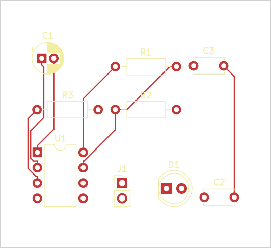
Smallest circuit that exercises the whole pipeline end-to-end: a classic NE555 astable that flashes an LED at ~1 Hz. Not meant to be useful — meant to prove the toolchain works.
- Components
- 9
- Copper
- 2-layer
- Area
- 1856 mm²
- Routing
- 65 seg · 0 via
- DRC
- —
- Fab
- ready
USB-C 3.3 V LDO
SMD · power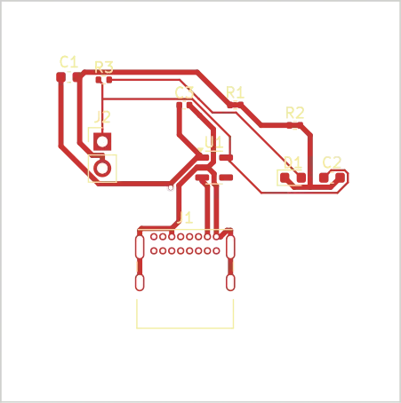
5 V in over a USB-C receptacle → clean 3.3 V out via an AP2112K-3.3 LDO at up to 600 mA. First board with real power topology, a USB-C pinout, and a regulator IC instead of a 555.
- Components
- 10
- Copper
- 2-layer
- Area
- 1467 mm²
- Routing
- 102 seg · 1 via
- DRC
- clean
- Fab
- ready
FPV Flight Controller
STM32F411 · 2-layer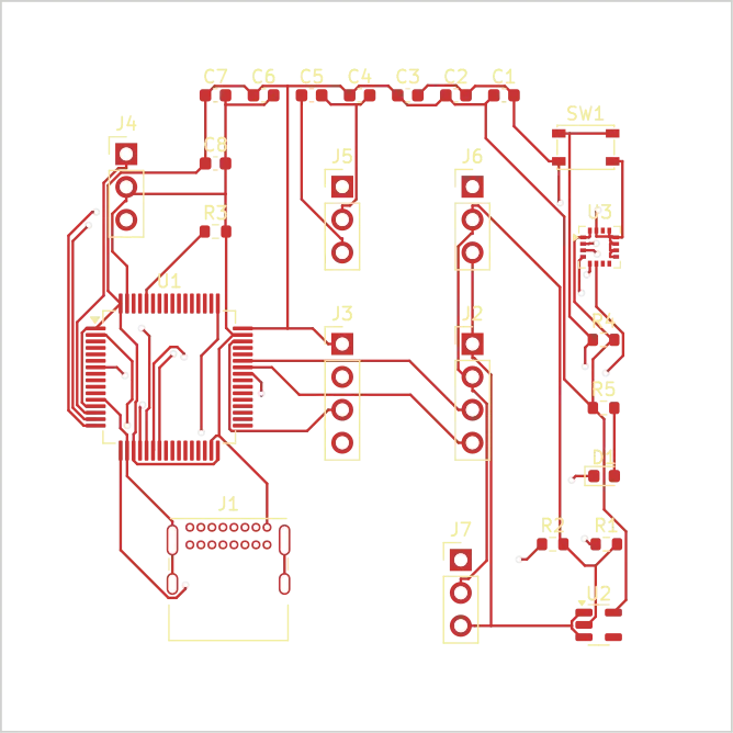
First microcontroller-class board: an all-in-one FPV flight controller around an STM32F411, a SPI IMU (ICM-20602), and four PWM ESC outputs. The real test of whether the pipeline handles pin-assignment constraints at ~25 components.
- Components
- 25
- Copper
- 2-layer
- Area
- 3197 mm²
- Routing
- 374 seg · 22 via
- DRC
- clean
- Fab
- ready
Flight-Ready FC
STM32F411 · 4-layer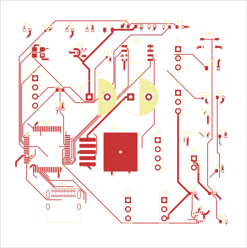
The fc_basic flight controller scaled up for actual flight: 2S–4S Li-Po battery input with a buck converter, an 8 MHz HSE crystal, and SPI flash — 41 components on a 4-layer stack with dedicated GND and 3V3 inner planes.
- Components
- 41
- Copper
- 4-layer +planes
- Area
- 4731 mm²
- Routing
- 2 unrouted
- DRC
- 32 errors
- Fab
- in progress
The honest one is fc_full. At 41 components on four layers it's where
the pipeline starts to strain: a couple of fine-pitch nets on the
LGA-class footprints don't escape cleanly yet, so it lands with two
unrouted nets and DRC errors instead of a fab-ready zip. That's the
current edge of the envelope, and it's left visible rather than hidden.
Closing the loop
Placement is where an LLM's lack of spatial reasoning hurts most — so
instead of trusting it to place well, the pipeline lets it critique.
A vision model looks at the rendered board, emits placement constraints
(near / edge / separate / align), a simulated-annealing placer
moves the parts to satisfy them, FreeRouting re-routes, and the cycle
repeats. Joint-metric rollback rejects any iteration that regresses
wirelength, via count, or unrouted nets, so the board can only improve
or hold.
usb_ldo · wirelength fell 25% and vias went to zero before the joint metric stopped improving. One AI-in-the-loop run on the USB-C LDO. A vision LLM reads the rendered board and emits placement constraints; a simulated-annealing placer minimizes a joint cost; FreeRouting re-routes; repeat. Joint-metric rollback rejects any iteration that regresses wirelength, vias, or unrouted-net count — so the board can only get better or stay put.
Every iteration also appends a full footprint-state row to a trace file. That trace is the training corpus for the longer-term plan: replace the LLM critic with a GNN/RL placer that has native spatial reasoning, trained on the pipeline's own runs.
How it works
- Intent → circuit
- LLM · few-shot + ERC auto-fix
- Circuit DSL
- SKiDL (hardware-as-code)
- EDA
- KiCad 9 · kinet2pcb · pcbnew
- Routing
- FreeRouting via DSN/SES
- Critique
- Vision LLM → constraint JSON
- Placement
- Simulated annealing · joint cost
- Stackup
- 2 / 4 / 6 / 8 layer · GND+3V3 planes
- Output
- Gerbers · drill · BOM · pick-and-place
Current state
v0.8 — the full intent → AI-optimized, multi-layer, fab-ready path
works end to end. Three of the four reference boards export clean,
DRC-passing Gerber packages; the densest one exposes the LGA fine-pitch
fanout as the next real problem to solve. Backends span free local
Ollama, cheap OpenRouter coding models, and the Anthropic API for the
hard boards.
What's next
Two threads. Fanout — proper escape patterns for fine-pitch LGA/QFN footprints so dense boards stop leaving unconnected pads. A learned placer — train a GNN or RL placement model on the accumulated optimization traces to replace the vision-LLM critic with something that reasons about geometry directly, which is the part of the problem that language models will probably never own.
∴⎯Related work